Over the past couple of months, there's been quite an uproar on various tech forums about Samsung's latest 30 nm Low-Power "Green" DDR3. During the time since they were "discovered", we've seen reports of 1600 MHz sticks hitting 2400 MHz and more, a healthy 50%+ overclock ability that in today's memory market is very near unheard of. Non-plussed, I managed to source a sample to take a look, and investigate the hype. Here's what Samsung has to say about their latest Low Power "Green" DDR3 on their website:

Double Data Rate Three, Synchronous DRAM, or DDR3, is the new generation of high performance, ultra-low-power memory interface technology used in high performance servers, desktops and notebooks. As the number one supplier in memory, Samsung continues to lead the industry with cutting-edge SDRAM products from the first DDR in 1997, DDR2 in 2001 and DDR3 in 2005. Samsung's high performance main memory solutions are based on JEDEC standards and leverage the company's leadership in advanced research and development of semiconductor process technology.
Samsung's DDR3 brings new levels of performance to notebooks, desktops and servers and pushes the envelope in key areas like power consumption, speed and bandwidth. Our recent 30nm class, 1.35V, 2Gb DDR3 is the world's first ultra-low-power memory technology, with more than a 76% power savings over traditional DDR2 at 2x the bandwidth. When you're ready to make a move to DDR3 or are considering upgrading your systems, we're here to provide the best optimal solution for enhancing your competitive edge.
As far as I am aware of, Samsung hasn't had a memory product that excited enthusiasts since the release of their 1.8v HCF0 ICs, which although decent overclockers, were eclipsed by other products on the market that went just that much further. Of course, those HCF0 weren't 30nm, nor were they rated for operation at 1.35 V. Are these new sticks worth the hype the receive?

Packaging

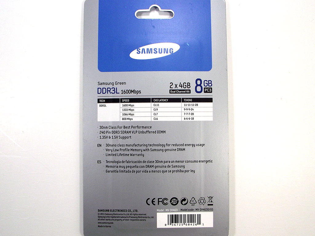
The Samsung MV-3V4G3D/US kit showed up on my doorstep after a trip
across the ocean, clad in paper-based packaging that is nearly 100%
recyclable. The grey and blue colors used on the package are commonly
seen on quite a few Samsung products, and help make them easy to notice
on the store shelf. There is very little text on the front of the box,
with just the important details shown, Green DDR3 for Desktop use, 8 GB
in a 2x 4 GB configuration, 1600 Mbps, and 30nm Class Low Voltage.
Looking at the rear of the packaging, we find a listing of the different
modules you can buy, and the timings for each model (higher-rated
modules are compatible with lower speeds and timings, although,
according to Samsung, they have not been tested at those lower speeds).


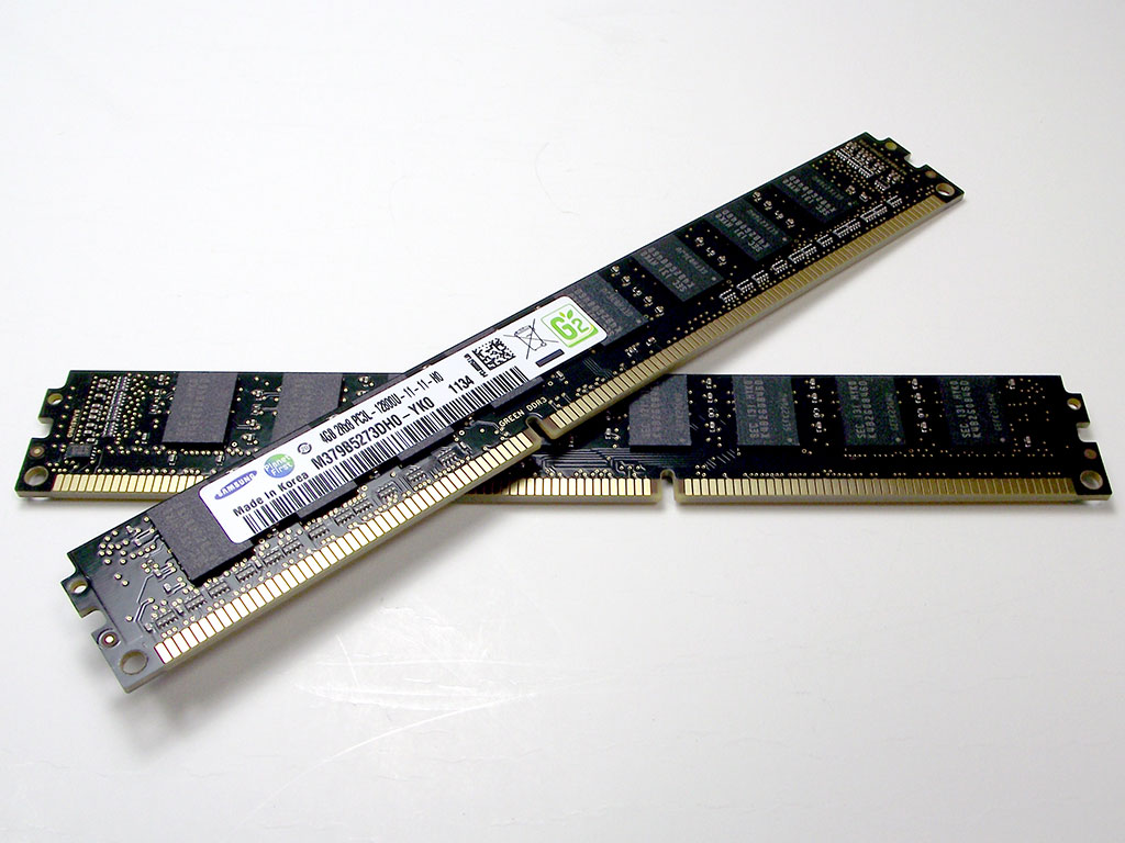
Opening the packaging was a bit more difficult than what I am used to,
as seen in the first image above. There is a bare minimum of plastic
used, and it is very deftly embedded into the paper in such a way that
getting out the modules requires destroying the packaging completely. I
personally like to keep all of my product packaging, so this was a bit
upsetting, but it is just the packaging, so nothing to be too concerned
about, now is it?
Once I had the modules out, I also found a little paper installation guide along with the modules themselves. It was folded into a small little bundle that fit neatly behind one the DIMMs, and even though I ripped the package open, it managed to stay intact. The engineers that design Samsung's packaging surely earns their wages!
The modules themselves are dual-sided sticks with eight memory ICs per side, mated with a nice black PCB, that is more often than not reserved for much more expensive modules. The very low asking price for these modules, even directly via Samsung's website, betrays the true potential these sticks have, and that was very evident once the modules were in my tech-loving hands. Let's take a closer look.
A Closer Look
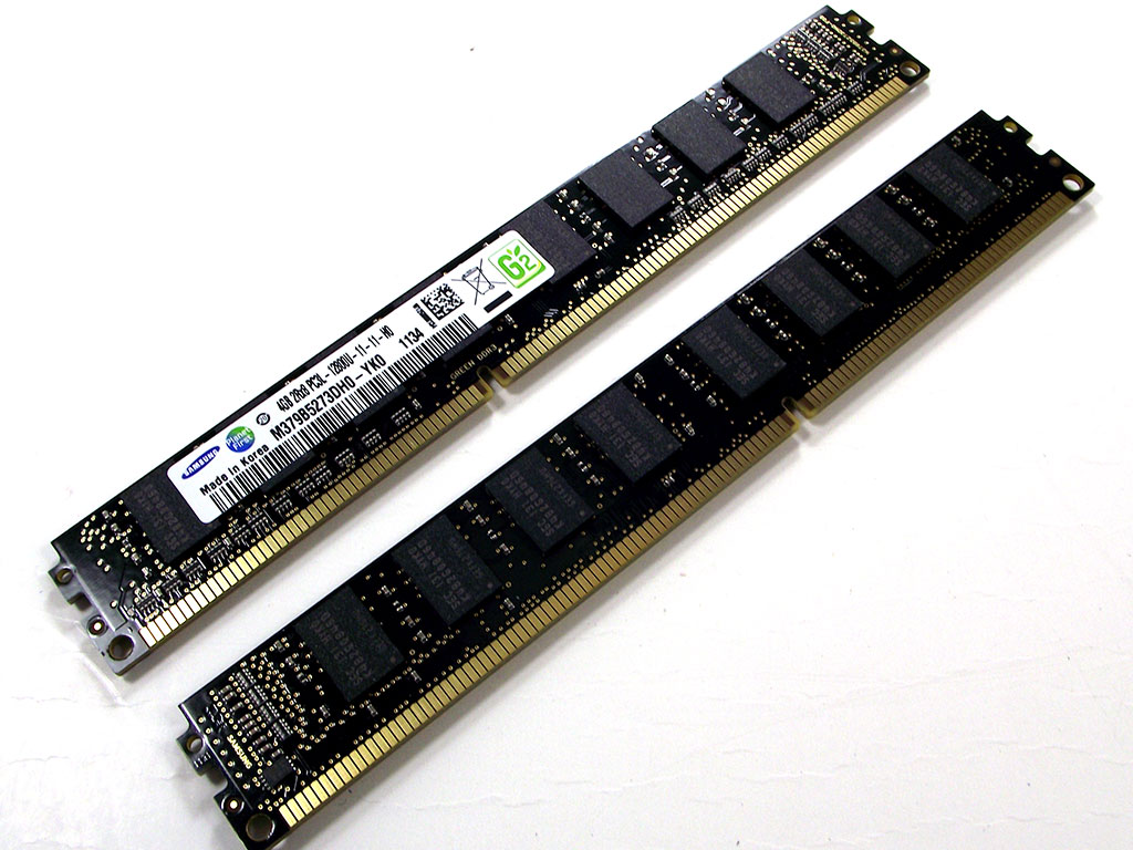

With all the modules out of the packaging, we can see them all clearly,
and I noticed that although the appearance of each side of the DIMMs is
different at first glance; this is just due to the sticker with the
module specifications on one side. With the modules inserted into the
slot, the sticker is on the side that faces away from the CPU socket
itself, not exactly my most favorite orientation, but it works fine. As
you can see in the images above, these sticks differ a bit from other
sticks, in that the ICs themselves are offset to one side of the DIMM,
rather than evenly spaced. It's pretty obvious when you see the sticks
as they are in the second image above.


The modules don't have very many surface-mounted parts, and I didn't
notice the SPD ROM at first either, but it's hidden under the stick's
label.


Looking at the DIMM from top and bottom, it's pretty clear that this PCB
is probably nearly as optimized as is possible, with barely a
millimeter or two of PCB sticking out above the top of the memory ICs.
The short PCB allows for much shorter traces in the PCB itself, which
should help with overclocking and stability.
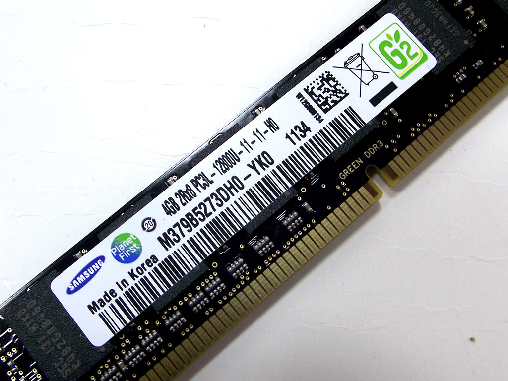
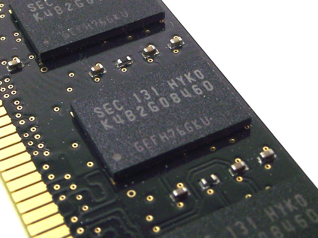
The label on the sticks doesn't disclose a lot of information, but we do see size and latencies noted. The ICs themselves are genuine Samsung 30nm "HYK0"-grade parts, with a part number of "K4B2G08460". The darker-grey lettering across the bottom of the IC itself is a batch code, and other than that, there are very few physical characteristics that help distinguish this IC from others, although the physical dimensions, of course, can be quite useful.
Test System
| Test System | |
|---|---|
| CPU: | Intel i7 3960X (ES) 3.3 GHz, 15 MB Cache |
| Memory: | 8 GB DDR3 (2x 4 GB) Samsung MV-3V4G3 |
| Cooling: | Noctua NH-C14 |
| Motherboard: | ASUS P9X79 Deluxe Intel X79 Express, BIOS ver 0904 |
| Video Card: | XFX Radeon HD 6950 2 GB(shader unlocked) |
| Harddisk: | Corsair CSSD-F60 60GB SATA 3 Gb/s Crucial CT128M4SSD2 128GB SATA 6 Gb/s |
| Power Supply: | Antec TPQ-1200 OC |
| Case: | Test Bench |
| Software: | Windows 7 64-bit, ATI Catalyst 12.1 |
Initial Setup
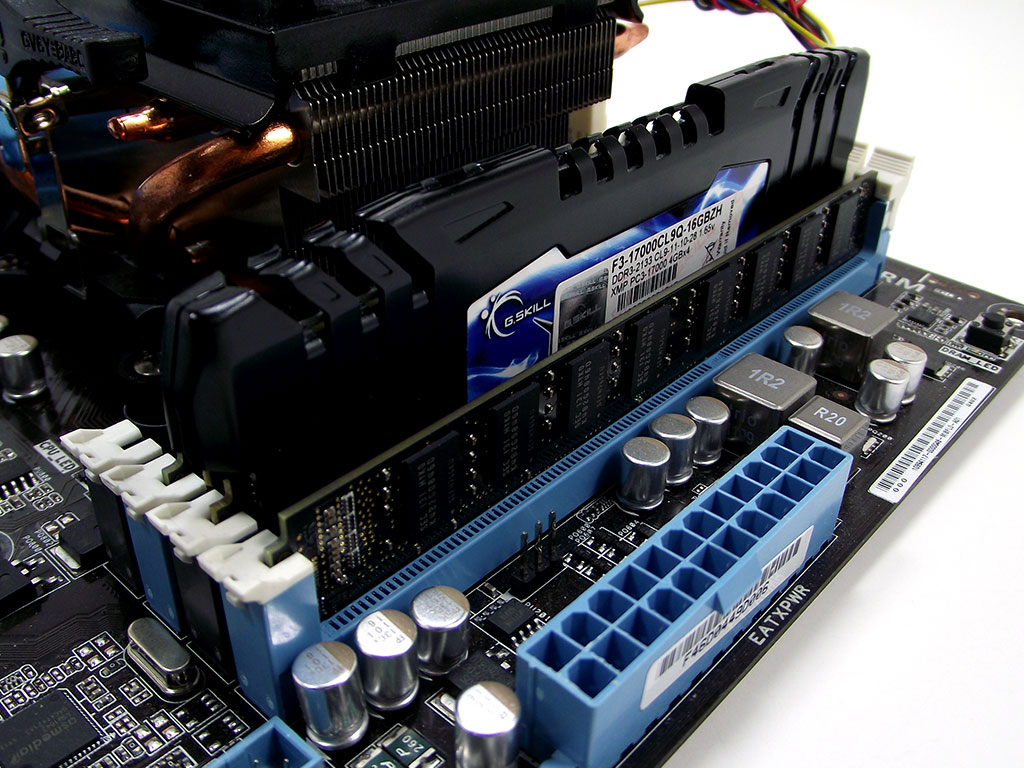


I installed the sticks next to the G.Skill memory I reviewed several weeks ago, and as you can see in the first image above, that really helped highlight just how small these sticks are! In the second image we can see that the Samsung sticks are about half the height of the G.Skill sticks, which already easily fit under our standard NH-C14 Noctua cooler that we use in all of our reviews.
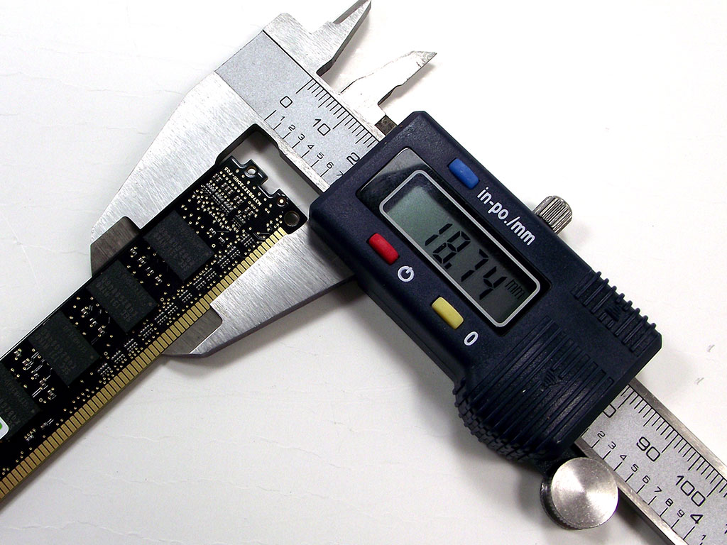

The modules measure in at 18.74 mm in height; quite small indeed. So small in fact, that these modules barely even stick out past the DIMM slot clips, as you can see in the second image above.

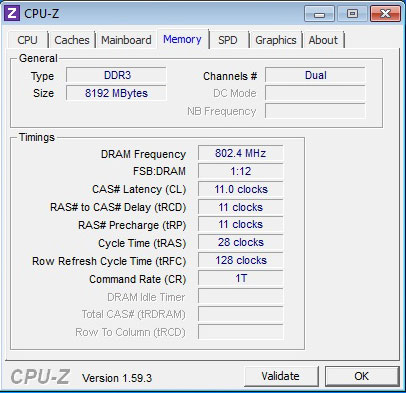
Once in the OS, I fired up CPU-Z to see what info would be displayed, which you can see in the two images above. It's interesting to note that CPU-Z recognizes the sticks as having a 1.28 V working voltage.
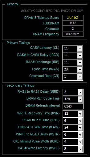

The two images above show the timings and voltages the sticks use by default in our ASUS P9X79 Deluxe motherboard. Secondary timings perfectly match what we found in the SPD table (not all sticks get the same settings as what's in the SPD profile), and the second image above shows that even with "AUTO" voltage settings, the dimms were set to 1.35 V, and VCCSA was not adjusted at all (our reference G.Skill kit set 1.05 V for VCCSA when XMP was enabled, as well as using 1.65 V for vDIMM on "AUTO" settings, even with the JEDEC profile).
Performance Results


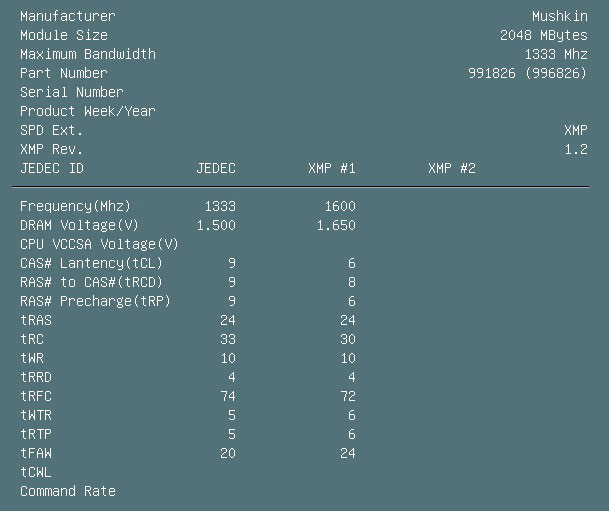
The above three images are screen captures from within the ASUS P9X79 Deluxe's BIOS. The first image shows the Samsung module's offered profiles, including the primary as well as secondary timings that the module uses depending on which profile is enabled. This handy screen can help users manually set timings, but it's also worth mentioning that simply selecting and enabling "XMP" in the ASUS BIOS will automatically set most of these timings, but we did find that a few of the timings were different than what is reported in the screens above with some sticks. I've also included the same screenshot from the G.Skill and Mushkin sticks, so we can see the obvious differences and similarities in timings.
My testing involves using only the automatic settings applied by the BIOS, as this is what most users will do as well, so the results that follow should be able to be replicated by anyone with the same components. I have tested the different modules with the primary JEDEC profile, as well as the XMP profile for sticks that offer it, and the results are below. The numbers below reflect performance results with two modules installed for the Samsung kit, and four sticks for the other two kits.
SuperPi

SuperPi has been a standard in memory clocking in enthusiast circles for many, many years. Being highly sensitive to timing and speed adjustments both on the CPU and on the memory, SuperPi is also good for stability testing for those just benchmarking. The Samsung MV-3V4G3 sticks ended up on the bottom of the pile here, but perhaps there's more to them than this one test shows.
wPrime

wPrime is much more focused on CPU performance, but memory plays a role too, although timings are far more critical. Here, the Samsung memory is just ahead of the other memory kits, but performance still remains fairly close even with the vastly different speeds and timings between all the kits.
WinRAR

WinRAR makes use of both CPU and memory again, and the test results highlight how perhaps quad-channel mode can be a hinderance to performance. The Samsung kit, with its JEDEC profile, is half-way between the other JEDEC scores, and the XMP scores, showing that WinRAR seems to prefer dual-channel mode on the X79 platform.
AIDA64 Read Performance

Memory adjustments on the X79 platform affect Read performance more than Copy and Write performance. Here the JEDEC and XMP profiles put the G.Skill kit ahead of the Mushkin kit by roughly 700 MB/s in the AIDA 64 Read Performance test, even though AIDA 64's tests don't fully utilize all four channels on the Intel X79 Express platform. However, the Dual-Channel Samsung kit beat both of the other JEDEC profiles, which really does seem to bolster the idea that these tests may not reflect performance fully. Thankfully, I ran many more tests.
AIDA64 Latency Performance

The gains in latency are pretty linear too, with the Samsung MV-3V4G3 kit winning out between the JEDEC profiles again. This is more than likely due to the lower tRC value the Samsung sticks use.
SiSoft Sandra Bandwidth Performance

SiSoft Sandra's memory test suite provides a slightly different workload than the AIDA 64 tests do, so we've employed it for testing too. With all four channels used, the performance gaps become much larger overall, and the Samsung kit takes the bottom spot. Although it's on bottom, it's using 50% less sticks, but offering more than 50% of quad-channel performance. Interesting result.
SiSoft Sandra Latency Performance

Latency Performance in SiSoft Sandra closely follows the trend seen in AIDA 64 with quad-channel kits, but again we are left with a different result from using just two sticks, Leaving the Samsung kit over 200% faster than all the other kits in this test. Quite amazing.
SiSoft Sandra Cache Performance

The SiSoft Sandra Cache test works not only the memory, but also the CPU cache, highlighting how memory performance affects not just the memory itself, but also how your CPU operates. The Samsung kit, with two less sticks, and two less channels active, put out pretty significant results, almost catching the four Mushkin sticks at 1333 MHz.
HandBrake Encoding

Handbrake encoding testing followed the results given by wPrime, showing that sometimes timings are more important, but not always. Again the Samsung kit wins out of all the JEDEC profiles.
CineBench Encoding

Cinebench encoding, on the other hand, provides a much different encoding workload, where it seems raw speed wins out overall. Samsung MV-3V4G3 kit is again on top, without a doubt.
PCMark 7

PCMark7 provides a bit of a daily usage comparison, testing different parts of the system in different ways. Even in daily performance testing, the Samsung MV-3V4G3 wins out of all the JEDEC profiles, but only marginally so.
Shogun 2 CPU Bench

We fired up the Shogun 2 DirectX 9 CPU Performance Benchmark for some game workload testing. We've updated all of our test results because previously we used an HIS HD5450 for testing memory, but we found that the results given might be a bit VGA-limited. With an XFX HD6950 2 GB card installed, we get a much better picture of what's going on, and although the Samsung kit is not the best JEDEC result, it is fairly close to even the XMP profiles we tested!
This group of tests has enlightened me to what a lot of other reviewers are saying: Quad Channel memory might be hindering the X79 Express paltform's performance in many apps. At the same time, these results might help some users who are wondering about re-using an existing Dual-Channel kit; I really have to say I cannot tell much difference between dual- and quad-channel during daily usage at all, as long as the Dual-Channel kit has adequate capacity.
Overclocking
Overclocking the Samsung 30nm MV-3V4G3 sticks proved very rewarding. With only adjustments to the voltage and secondary timings, I easily reached 2400 MHz with 11-11-11-28-1T timings. Full stability did, however, require 1.575 V, which is a fair bit outside of what I would consider the "comfort zone" for these sticks. Adding voltage did not offer much in the way of frequency increases, as we easily passed 2000 MHz with the stock 1.35 V with default primary timings, and any overclock with adjusted primary timings met with very miniscule gains from 1.35 V to 1.55 V, with an average of about 25 MHz for each 0.1 V of additional voltage supplied. With the default 11-11-11-28 primary timings, we saw near 100 MHz increases with each 0.1 V additional applied to the sticks. A loss of 75 MHz in frequency because of timing changes is something that just cannot be ignored.An overclocking tidbit or two for those with these sticks:
Timing programming:

There are two timings that are linked together that will help greatly in overclocking. When these two timings are not set correctly, overclocking will not be as successful, and long-term stability can be hard to attain without excessive voltage. The above picture shows the primary and secondary timings we used to reach 2400 MHz with 1.575 V.
The two crucial timings, of course, are CAS Latency, and Write CAS Latency.
For CAS 6 and 7, tWCL should be CAS -1 (so CAS 6 gets tWCL 5 and CAS 7 gets tWCL 6)
For CAS 8 and 9, tWCL should be CAS -2 (so CAS 8 gets tWCL 6 and CAS 9 gets tWCL 7)
For CAS 10 and 11, tWCL should be CAS -3 (so CAS 10 gets tWCL 7, and CAS 11 gets tWCL 8)
I mention this as tWCL is not a timing that is talked about very often, if at all. However, because it has proven itself as a critical timing during testing, it is something that I felt must mention.
Voltage Scaling:
The 30 nm memory ICs are manufactured by Samsung, commonly referred to as "D-die" and have two voltage modes, 1.35 V, and 1.5 V. The two different voltage modes and supporting DIMMs do use the same memory IC, so attempting to use the higher voltage setting on 1.35 V sticks maybe provides some success when overclocking, but seemingly the low-profile PCB prefers 1.35 V, and the "regular" PCB prefers 1.5 V. Both types can be purchased currently at very low prices.
The 1.35 V and 1.5 V settings each have pre-specified limits, with 1.35 V supporting 1.28 V - 1.475 V, while the 1.5 V mode supports 1.45 V - 1.575 V. I have found that the 1.35 V mode does operate at lower voltages as well, but going lower than 1.25 V can cause artifacting on the desktop with certain VGAs, even though stability testing passes with flying colors.
That said, I was able to run the default 11-11-11-28-1T timings @ 1600 MHz with just 1.2 V, which is considerably lower than the stock 1.35 V.
I also found that adjusting voltage outside of the pre-programmed voltage mode results in frequency scaling dropping off quite quickly as explained above, so I recommend that users do not exceed the pre-determined voltage ranges in order to prolong the DIMM's life. That means that 1.35V sticks should see no more than 1.475 V, and 1.5 V sticks should see no more than 1.575 V. Both types of DIMMs do seem to scale a little bit once those values have been exceeded, but because the gains are quite minimal, it is not recommended at this time.
Overclocked Performance Summary

SuperPi showed to be nearly 19 seconds faster using the overclocked settings, and the same CPU speed.

wPrime got a decent bopost as well, nearly seven and a half seconds.

AIDA Read Performance got close to a 4000 MB/s boost, and surpassed the G.Skill kit at the same speed.

Latency improved by 12.5 ns, a huge boost to performance.

WinRAR also got a good boost, again outclassing the G.Skill kit.

Shogun 2 finally showed decent gains, but did not allow the Samsung MV-3V4G3 to really beat out the G.Skill kit.
Timing and Frequency Scaling
Part of my testing routine involves testing memory samples using a variety of common timings and voltages, in order to judge the flexibility of the modules to match system overclocks. I test Low Voltage DIMMs using three different voltage levels: 1.35 V, the standard JEDEC voltage, 1.45 V, for common voltage scaling, and 1.55 V, for a max OC overvoltage setting. I set the timings for the memory and measure the maximum frequency with each voltage, and then adjust the timings and test again. I employ several tests to measure the performance differences, including AIDA64's built-in memory benchmark, 3DMark 2001, SuperPi v1.55 32M, as well as the RTS game Shogun 2, for some memory-sensitive 3D performance. I also swapped out the HIS Radeon HD 5450 1GB card used in the last review for an XFX HD 6950 2 GB card, in order to eliminate bottlenecks in performance introduced by the videocard.Clocking memory on the Intel X79 Express platform can provide some very interesting results, thanks to the introduction of higher memory frequency dividers as well as BCLK dividers, which allow for higher memory clocking than on any previous Intel platform. On Intel Socket 1155 products, BCLK scaling is very limited, with 104 MHz being the average maximum BCLK reported by users over the past 12 months since the Intel P67 Express platform launch. Intel's X79 Express platform expands upon its predecessor by adding both 125 MHz and 166 MHz BCLK dividers, which allow the bus to clock a lot higher. Effectively this divider de-couples the PCIe bus from the BCLK, allowing the ratio between BCLK and PCIe to be adjusted, providing for greater flexibility. Naturally, with a 125 MHz BCLK matched with a 100 MHz PCIe clock, the BLCK can be adjusted in a wider range before pushing the PCIe bus outside of the range of stability, as rather than each MHz in BCLK adjustment moving the PCIe bus by the same increment, one MHz of BLCK adjustment now moves the PCIe bus just 0.8 MHz.
It's important to note that different devices on the PCIe bus have different clock tolerances, and therefore onboard devices that use the PCIe bus can greatly affect how far the BCLK can go. Due to the use of parts common to both SKT 1155 and SKT 2011, the 100 MHz BCLK divider on SKT 2011 doesn't really offer greater flexibility than on SKT 1155, so for greater clock scaling, we employ the 125 MHz BCLK divider whenever possible, and also adjust the CPU multiplier to try to match the same CPU speed for all tests, but as the BLCK used can vary according to the maximum stable memory frequency, so can the CPU speed. For our testing we have kept the CPU speed between 4.0 GHz and 4.1 GHz. The numbers provided within each CAS setting are meant as a reference only, although overall the results do reflect performance increases based on memory performance alone.
Of course, because the PCIe bus still plays a role in the final effective BLCK speed, there are times where FSB "holes" are introduced, as our particular CPU, VGA, and board combination has an effective range of 100 MHz to 105 MHz using the 100 MHz divider, and 113 MHz to 134 MHz using the 125 MHz divider. For example, using the 1066 MHz memory divider and a 133 MHz BCLK results in a 1418 MHz effective memory speed. Dropping the BCLK down to 113 MHz with the 1333 MHz memory divider results in 1506 MHz, so there is a 86 MHz hole in the effective memory speed that just cannot be attained no matter what modules are used.


While clocking the Samsung MV-3V4G3D/US kit, I found 1.35 V to be the optimal voltage, allowing the frequency to scale all the way up to 2080 MHz. We found two optimal settings; the first using 9-9-9-27, @ 1.35 V, and 1866 MHz on the memory, and second, 1.45 V and 2133 MHz, with the default 11-11-11-28 timings. A full 1.45 V was not required for 2133 MHz to be fully stable, and did allow for an additional 68 MHz in memory speed, but this particular setting is great when matched with a small BLCK overclock on the 100 MHz divider, while using the 2133 MHz memory setting. We did also test higher voltages, all the way up to 1.75 V, but due to the small gains offered at lower speeds and timings, we find it ill advised to use so much voltage on these sticks, considering the minimal performance gains offered. Our CPU is incapable of surpassing 2400 MHz it seems, as we were unable to test much higher than we reached with just 1.55 V, but it's absolutely amazing to see such an in-expensive Low-Voltage kit completely max out our CPU, reaching to 50% overclock without breaking a sweat.
Value & Conclusion
 |
|
|---|---|
 |
|
 |
|
I really cannot say enough good things about this kit from Samsung. It
easily beat our expectations, and managed not only to outperform the
other kits on JEDEC settings, but also did it while using less power!
The overclocking potential of these sticks is huge, and again, they
manage to clock sky high, using less voltage than many other kits that
are exponentially more expensive.
Our testing even proved to show that there are significant gains to be had using Dual-Channel memory on the Intel X79 Express platform in some instances, rather than quad-channel, which was quite surprising to say the least. I have been recommending these sticks since I got them, and I am sure to continue to do so for some time yet. Admittedly, they aren't the most aesthetically pleasing of sticks, but at the same time, there's literally no chance that this kit is going to interfere with ANY aftermarketing cooler, now, or in the future, thanks to their compact size. With all things considered, Don't forget to hit us up in the forums for help getting your kit running the best it can!