Pages

Showing posts with label AMD. Show all posts

09 March 2012

AMD Radeon HD 7850 & HD 7870 2 GB

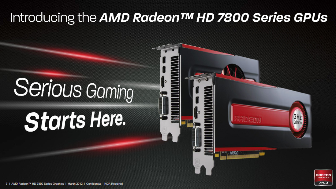
Introducing AMD Radeon HD 7850 & HD 7870 2 GB


"Next-generation", "Graphics CoreNext", "Radeon HD 7000 series", "Southern Islands"...this is it. AMD's new GPU architecture has moved into the phase where its makers launch serious money-making products based on it, with the Radeon HD 7800 series.


Targeting a wide price-range between $250-$350, the HD 7800 series falls into the market-segment both AMD and NVIDIA have known to refer to as the "sweetspot" segment. When people decide to turn their $400 Dell desktops into gaming PCs, instead of buying $300 game consoles for their TV, it's graphics cards from this segment that they end up buying. Smooth gameplay at full-HD resolution is a requisite.

AMD has to get several things right about the products it's launching today, because the competitiveness of the entire HD 7000 series hangs on its success. First, it needs to create a sizable performance jump, over the previous-generation Radeon HD 6800 series; second, its new chip has to prove Graphics CoreNext as being a viable investment for AMD by meeting some basic cost/performance, performance/die-area, and performance/Watt figures. VLIW4 had a very short stint before Graphics CoreNext.


NVIDIA hasn't even started with its next-generation GPU lineup, leaving its previous-generation to defend itself against a reinvigorated AMD lineup. AMD appears to have exploited this late-coming by NVIDIA. The launch prices of Radeon HD 7900 series resembled those of NVIDIA's high-end GTX series, the Radeon HD 7700 series products ask a couple of dozen Dollars too many. AMD kept the theme going with the Radeon HD 7800 series. You may recollect AMD's Radeon HD 6870 shipping for $240 on launch, and the HD 6850 for $180, both very attractive prices. The slide above is every indication of AMD trying to justify launch prices of $349 for the HD 7870 and $249 for the HD 7850, just because they are touted to outperform whatever NVIDIA currently has in those price-ranges (we're going to find that out in this review).

Architecture

The Radeon HD 7800 series consists of two models, the Radeon HD 7870, and the Radeon HD 7850, both stretched far apart in the market segment. The two are based on AMD's brand new GPU, codenamed "Pitcairn". Built on the 28 nm fabrication process, this new chip holds 2.8 billion transistors. "Pitcairn" is a 100% upscale of the "Cape Verde" silicon, on which the Radeon HD 7700 series is based. It has 1280 Graphics CoreNext stream processors, arranged in 20 Graphics CoreNext Compute Units (GCN CUs). The component hierachy of "Pitcairn" resembles that of "Tahiti", more than it does "Cape Verde". The 20 GCN CUs are arranged in two clusters, with two sets of geometry processing engines, and rasterizers, handing the initial stages of graphics processing.

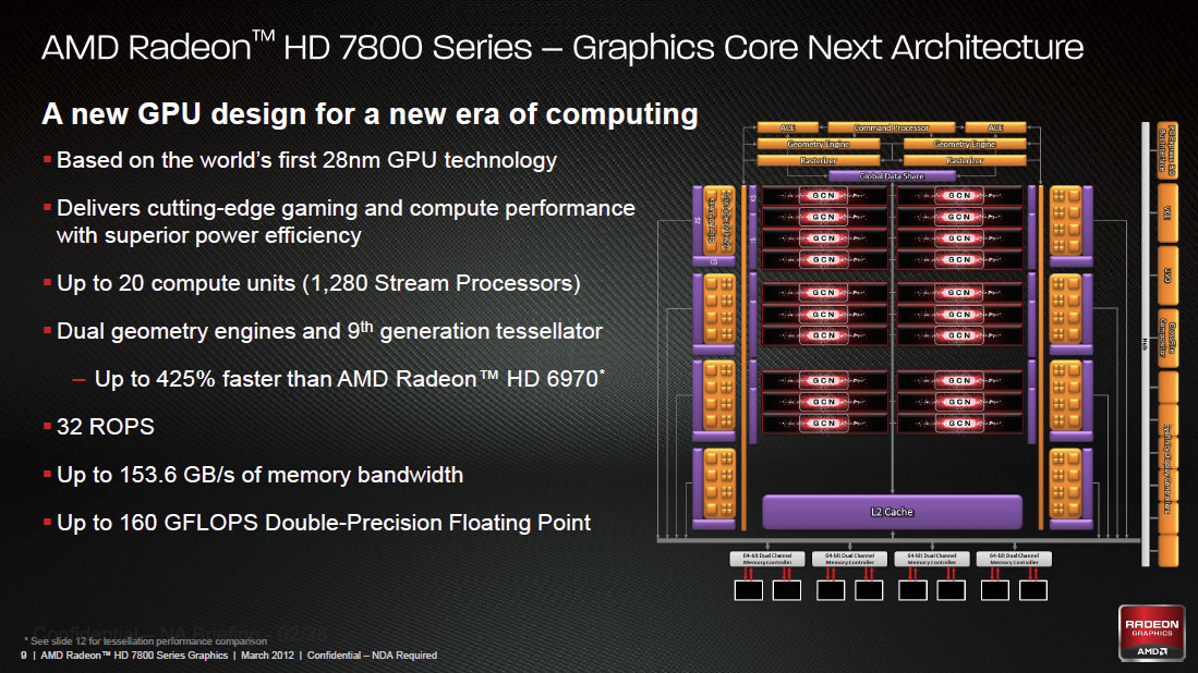
Apart from 1280 stream processors, Pitcairn has 80 Texture Memory Units (TMUs), 32 ROPs (Raster Operations), and a 256-bit wide GDDR5 memory interface, holding 2 GB of memory. Here's something interesting. AMD deemed 2 GB as the new standard memory amount for performance-segment graphics cards. Both the HD 7870 and HD 7850 have 2 GB of memory, clocked at 1200 MHz (4.80 GHz GDDR5 effective), churning out 153.6 GB/s memory bandwidth. As for the core clock, the HD 7870 has its core clocked at 1000 MHz, making it AMD's second "GHz Edition" SKU after the HD 7770; while the HD 7850 has its core clocked at 860 MHz. The Radeon HD 7850 is carved out by disabling four GCN CUs, leaving 1024 stream processors, and 64 TMUs. The rest of the SKU is identical to the HD 7870.

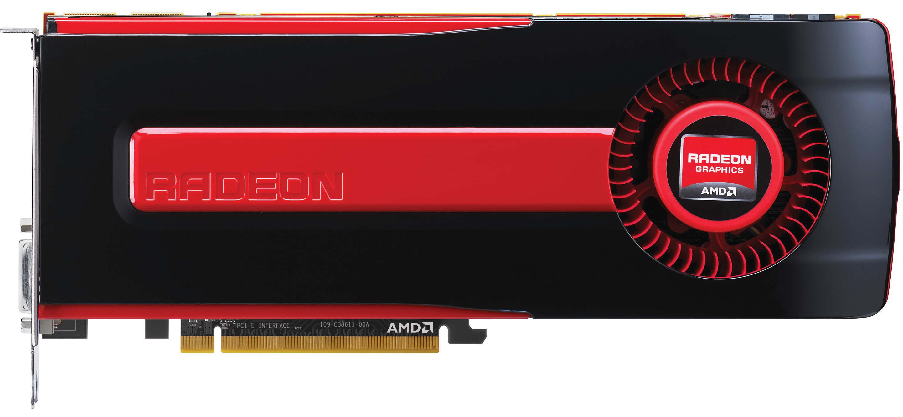
In this review, we are evaluating both the Radeon HD 7870 and the Radeon HD 7850. Both cards are AMD reference design samples provided by the company.

23 December 2011

AMD Radeon HD 7970 Review: 28nm And Graphics Core Next, Together As One


While AMD and NVIDIA are consistently revising their GPU architectures, for the most part the changes they make are just that: revisions. It’s only once in a great while that a GPU architecture is thrown out entirely, which makes the arrival of a new architecture a monumental occasion in the GPU industry. The last time we saw this happen was in 2006/2007, when unified shaders and DirectX 10 lead to AMD and NVIDIA developing brand new architectures for their GPUs. Since then there have been some important revisions such as AMD’s VLIW4 architecture and NVIDIA’s Fermi architecture, but so far nothing has quite compared to 2006/2007, until now.

At AMD’s Fusion Developer Summit 2011 AMD announced Graphics Core Next, their next-generation GPU architecture. GCN would be AMD’s Fermi moment, where AMD got serious about GPU computing and finally built an architecture that would serve as both a graphics workhorse and a computing workhorse. With the ever increasing costs of high-end GPU development it’s not enough to merely develop graphics GPUs, GPU developers must expand into GPU computing in order to capture the market share they need to live well into the future.

At the same time, by canceling their 32nm process TSMC has directed a lot of hype about future GPU development onto the 28nm process, where the next generation of GPUs would be developed. In an industry accustomed to rapid change and even more rapid improvement never before have GPU developers and their buyers had to wait a full 2 years for a new fabrication process to come online.

All of this has lead to a perfect storm of anticipation for what has become the Radeon HD 7970: not only is it the first video card based on a 28nm GPU, but it’s the first member of the Southern Islands and by extension the first video card to implement GCN. As a result the Radeon HD 7970 has a tough job to fill, as a gaming card it not only needs to deliver the next-generation performance gamers expect, but as the first GCN part it needs to prove that AMD’s GCN architecture is going to make them a competitor in the GPU computing space. Can the 7970 do all of these things and live up to the anticipation? Let’s find out…


The Radeon HD 7970 is a card of many firsts. It’s the first video card using a 28nm GPU. It’s the first card supporting Direct3D 11.1. It’s the first member of AMD’s new Southern Islands Family. And it’s the first video card implementing AMD’s Graphics Core Next architecture. All of these attributes combine to make the 7970 quite a different video card from any AMD video card before it.
Cutting right to the chase, the 7970 will serve as AMD’s flagship video card for the Southern Islands family. Based on a complete AMD Tahiti GPU, it has 2048 stream processors organized according to AMD’s new SIMD-based GCN architecture. With so many stream processors coupled with a 384bit GDDR5 memory bus, it’s no surprise that Tahiti is has the highest transistor count of any GPU yet: 4.31B transistors. Fabricated on TSMC’s new 28nm High-K process, this gives it a die size of 365mm2, making it only slightly smaller than AMD’s 40nm Cayman GPU at 389mm2.

Looking at specifications specific to the 7970, AMD will be clocking it at 925MHz, giving it 3.79TFLOPs of theoretical computing performance compared to 2.7TFLOPs under the much different VLIW4 architecture of the 6970. Meanwhile the wider 384bit GDDR5 memory bus for 7970 will be clocked at 1.375GHz (5.5GHz data rate), giving it 264GB/sec of memory bandwidth, a significant jump over the 176GB/sec of the 6970.


These functional units are joined by a number of other elements, including 8 ROP partitions that can process 32 ROPs per clock, 128 texture units divided up among 32 Compute Units (CUs), and a fixed function pipeline that contains a pair of AMD’s 9th generation geometry engines. Of course all of this hardware would normally take quite a bit of power to run, but thankfully power usage is kept in check by the advancements offered by TSMC’s 28nm process. AMD hasn’t provided us with an official typical board power, but we estimate it’s around 220W, with an absolute 250W PowerTune limit. Meanwhile idle power usage is looking particularly good, as thanks to AMD's further work on power savings their typical power consumption under idle is only 15W. And with AMD's new ZeroCore Power technology (more on that in a bit), idle power usage drops to an asbolutely miniscule 3W.

Overall for those of you looking for a quick summary of performance, the 7970 is quite powerful, but it may not be as powerful as you were expecting. Depending on the game being tested it’s anywhere between 5% and 35% faster than NVIDIA’s GeForce GTX 580, averaging 15% to 25% depending on the specific resolution in use. Furthermore thanks to TSMC’s 28nm process power usage is upwards of 50W lower than the GTX 580, but it’s still higher than the 6970 it replaces. As far as performance jumps go from new fabrication processes, this isn’t as big a leap as we’ve seen in the past.

In a significant departure from the launch of the Radeon HD 5870 and 4870, AMD will not be pricing the 7970 nearly as aggressively as those cards with its launch. The MSRP for the 7970 will be $550, a premium price befitting a premium card, but a price based almost exclusively on the competition (e.g. the GTX 580) rather than one that takes advantage of cheaper manufacturing costs to aggressively undercuts the competition. In time AMD needs to bring down the price of the card, but for the time being they will be charging a price premium reflecting the card’s status as the single-GPU king.

For those of you trying to decide whether to get a 7970, you will have some time to decide. This is a soft launch; AMD will not make the 7970 available until January 9th (the day before the Consumer Electronics Show), nearly 3 weeks from now. We don’t have any idea what the launch quantities will be like, but from what we hear TSMC’s 28nm process has finally reached reasonable yields, so AMD should be in a better position than the 5870 launch. The price premium on the card will also help taper demand side some, though even at $550 this won’t rule out the first batch of cards selling out.

Beyond January 9th, AMD as an entire family of Southern Islands video cards still to launch. AMD will reveal more about those in due time, but as with the Evergreen and Northern Islands families AMD has a plan to introduce a number of video cards over the next year. So 7970 is just the beginning.


16 November 2011

Five $160 To $240 990FX-Based Socket AM3+ Motherboards

Forty-two PCIe lanes give the 990FX a clear connectivity lead over competing Intel chipsets. We compare five class-leading products using AMD's FX-8150 to see which offers the best combination of performance, overclocking, integrated features, and value.
When it comes to the popularity of our stories, CPUs run second only to new graphics cards (which seem to get everyone's blood pumping the fastest). Motherboards fall behind quite a ways. That's a shame though, because the right board is an absolute necessity for connecting processors to GPUs, and every other components inside your machine.
This is where AMD gives a lot of love to its customers, whereas Intel tends to skimp more often. Nowhere is the difference between both company's mainstream parts more evident than in the chipset segment. The 990FX's 42 total PCIe 2.0 lanes provide a lot more potential throughput than Intel's popular Z68 Express, which is limited to 16 lanes from the CPU and a handful more on the Platform Controller Hub.
Of course, a fan of Intel's work could argue against the need for 42 lanes of second-gen PCIe when the 36 native to X58 Express support multi-card graphics configurations just as capably. But such a comparison really isn't necessary. After all, we've known for almost a year that Intel’s lower-cost Sandy Bridge-based part outperform the pricey six-core Gulftown-based processors in many desktop benchmarks, including pretty much every gaming scenario we throw at the two platforms.
And, it just so happens that Intel's mainstream (and multiplier-unlocked) Core i5 and Core i7 chips are more in the same league as AMD's most expensive enthusiast-oriented FX CPU.

The Importance Of PCIe

Gaming is where the Sandy Bridge architecture most easily proves that you don't need a thousand-dollar processor to turn in the best frame rates, and that's in spite of the 16 lanes built into each CPU's die. We've even seen situations where an NF200 bridge soldered down onto a Sandy Bridge-based motherboard enables performance just as compelling as a high-end LGA 1366 configuration. The thing is, a Z68 or P67 platform's 24 total PCIe 2.0 lanes aren't explicitly set aside for graphics cards. They have to handle every device attaching via PCI Express, including network and storage controllers.
We’ve even tested a few "enthusiast-class" Sandy Bridge-based motherboards so loaded with features that simply installing an add-in card forced certain slots or on-board controllers to become disabled. That doesn’t sound like a solution a power user would willingly accept to us.
As of this moment, enthusiasts who need more connectivity than the LGA 1155 platform offers are left to choose between “upgrading” to one of Intel’s older LGA 1366 platforms, paying extra for a motherboard with bandwidth-sharing PCIe bridges, or shifting to a platform with more native PCI Express, a wider range of unlocked processors and prices, several times the reference clock overclocking headroom for locked processors, and a downright respectable chipset: AMD’s high-flying 990FX.