While AMD and NVIDIA are consistently revising their GPU architectures,
for the most part the changes they make are just that: revisions. It’s
only once in a great while that a GPU architecture is thrown out
entirely, which makes the arrival of a new architecture a monumental
occasion in the GPU industry. The last time we saw this happen was in
2006/2007, when unified shaders and DirectX 10 lead to AMD and NVIDIA
developing brand new architectures for their GPUs. Since then there have been some important revisions such as AMD’s VLIW4 architecture and NVIDIA’s Fermi architecture, but so far nothing has quite compared to 2006/2007, until now.
At AMD’s Fusion Developer Summit 2011 AMD announced Graphics Core Next,
their next-generation GPU architecture. GCN would be AMD’s Fermi
moment, where AMD got serious about GPU computing and finally built an
architecture that would serve as both a graphics workhorse and a
computing workhorse. With the ever increasing costs of high-end GPU
development it’s not enough to merely develop graphics GPUs, GPU
developers must expand into GPU computing in order to capture the market
share they need to live well into the future.
At the same time, by canceling their 32nm process TSMC has directed a
lot of hype about future GPU development onto the 28nm process, where
the next generation of GPUs would be developed. In an industry
accustomed to rapid change and even more rapid improvement never before
have GPU developers and their buyers had to wait a full 2 years for a
new fabrication process to come online.
All of this has lead to a perfect storm of anticipation for what has
become the Radeon HD 7970: not only is it the first video card based on a
28nm GPU, but it’s the first member of the Southern Islands and by
extension the first video card to implement GCN. As a result the Radeon
HD 7970 has a tough job to fill, as a gaming card it not only needs to
deliver the next-generation performance gamers expect, but as the first
GCN part it needs to prove that AMD’s GCN architecture is going to make
them a competitor in the GPU computing space. Can the 7970 do all of
these things and live up to the anticipation? Let’s find out…


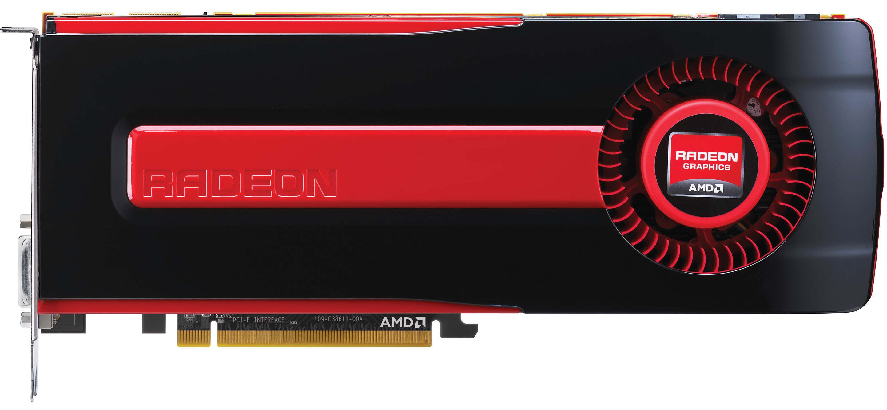
The Radeon HD 7970 is a card of many firsts. It’s the first video card using a 28nm GPU. It’s the first card supporting Direct3D 11.1. It’s the first member of AMD’s new Southern Islands Family. And it’s the first video card implementing AMD’s Graphics Core Next architecture. All of these attributes combine to make the 7970 quite a different video card from any AMD video card before it.
Cutting right to the chase, the 7970 will serve as AMD’s flagship video card for the Southern Islands family. Based on a complete AMD Tahiti GPU, it has 2048 stream processors organized according to AMD’s new SIMD-based GCN architecture. With so many stream processors coupled with a 384bit GDDR5 memory bus, it’s no surprise that Tahiti is has the highest transistor count of any GPU yet: 4.31B transistors. Fabricated on TSMC’s new 28nm High-K process, this gives it a die size of 365mm2, making it only slightly smaller than AMD’s 40nm Cayman GPU at 389mm2.
Looking at specifications specific to the 7970, AMD will be clocking it at 925MHz, giving it 3.79TFLOPs of theoretical computing performance compared to 2.7TFLOPs under the much different VLIW4 architecture of the 6970. Meanwhile the wider 384bit GDDR5 memory bus for 7970 will be clocked at 1.375GHz (5.5GHz data rate), giving it 264GB/sec of memory bandwidth, a significant jump over the 176GB/sec of the 6970.
These functional units are joined by a number of other elements, including 8 ROP partitions that can process 32 ROPs per clock, 128 texture units divided up among 32 Compute Units (CUs), and a fixed function pipeline that contains a pair of AMD’s 9th generation geometry engines. Of course all of this hardware would normally take quite a bit of power to run, but thankfully power usage is kept in check by the advancements offered by TSMC’s 28nm process. AMD hasn’t provided us with an official typical board power, but we estimate it’s around 220W, with an absolute 250W PowerTune limit. Meanwhile idle power usage is looking particularly good, as thanks to AMD's further work on power savings their typical power consumption under idle is only 15W. And with AMD's new ZeroCore Power technology (more on that in a bit), idle power usage drops to an asbolutely miniscule 3W.
Overall for those of you looking for a quick summary of performance, the 7970 is quite powerful, but it may not be as powerful as you were expecting. Depending on the game being tested it’s anywhere between 5% and 35% faster than NVIDIA’s GeForce GTX 580, averaging 15% to 25% depending on the specific resolution in use. Furthermore thanks to TSMC’s 28nm process power usage is upwards of 50W lower than the GTX 580, but it’s still higher than the 6970 it replaces. As far as performance jumps go from new fabrication processes, this isn’t as big a leap as we’ve seen in the past.
In a significant departure from the launch of the Radeon HD 5870 and 4870, AMD will not be pricing the 7970 nearly as aggressively as those cards with its launch. The MSRP for the 7970 will be $550, a premium price befitting a premium card, but a price based almost exclusively on the competition (e.g. the GTX 580) rather than one that takes advantage of cheaper manufacturing costs to aggressively undercuts the competition. In time AMD needs to bring down the price of the card, but for the time being they will be charging a price premium reflecting the card’s status as the single-GPU king.
For those of you trying to decide whether to get a 7970, you will have some time to decide. This is a soft launch; AMD will not make the 7970 available until January 9th (the day before the Consumer Electronics Show), nearly 3 weeks from now. We don’t have any idea what the launch quantities will be like, but from what we hear TSMC’s 28nm process has finally reached reasonable yields, so AMD should be in a better position than the 5870 launch. The price premium on the card will also help taper demand side some, though even at $550 this won’t rule out the first batch of cards selling out.
Beyond January 9th, AMD as an entire family of Southern Islands video cards still to launch. AMD will reveal more about those in due time, but as with the Evergreen and Northern Islands families AMD has a plan to introduce a number of video cards over the next year. So 7970 is just the beginning.

A Quick Refresher: Graphics Core Next
One of the things we’ve seen as a result of the shift from pure
graphics GPUs to mixed graphics and compute GPUs is how NVIDIA and AMD
go about making their announcements and courting developers. With
graphics GPUs there was no great need to discuss products or
architectures ahead of time; a few choice developers would get
engineering sample hardware a few months early, and everyone else would
wait for the actual product launch. With the inclusion of compute
capabilities however comes the need to approach launches in a different
manner, a more CPU-like manner.
As a result both NVIDIA and AMD have begun revealing their
architectures to developers roughly six months before the first products
launch. This is very similar to how CPU launches are handled, where the
basic principles of an architecture are publically disclosed months in
advance. All of this is necessary as the compute (and specifically, HPC)
development pipeline is far more focused on optimizing code around a
specific architecture in order to maximize performance; whereas graphics
development is still fairly abstracted by APIs, compute developers want
to get down and dirty, and to do that they need to know as much about
new architectures as possible as soon as possible.
It’s for these reasons that AMD announced Graphics Core Next, the fundamental architecture behind AMD’s new GPUs, back in June of this year
at the AMD Fusion Developers Summit. There are some implementation and
product specific details that we haven’t known until now, and of course
very little was revealed about GCN’s graphics capabilities, but
otherwise on the compute side AMD is delivering on exactly what they
promised 6 months ago.
Since we’ve already covered the fundamentals of GCN in our GCN preview
and the Radeon HD 7970 is primarily a gaming product we’re not going to
go over GCN in depth here, but I’d encourage you to read our preview to
fully understand the intricacies of GCN. But if you’re not interested in
that, here’s a quick refresher on GCN with details pertinent to the
7970.
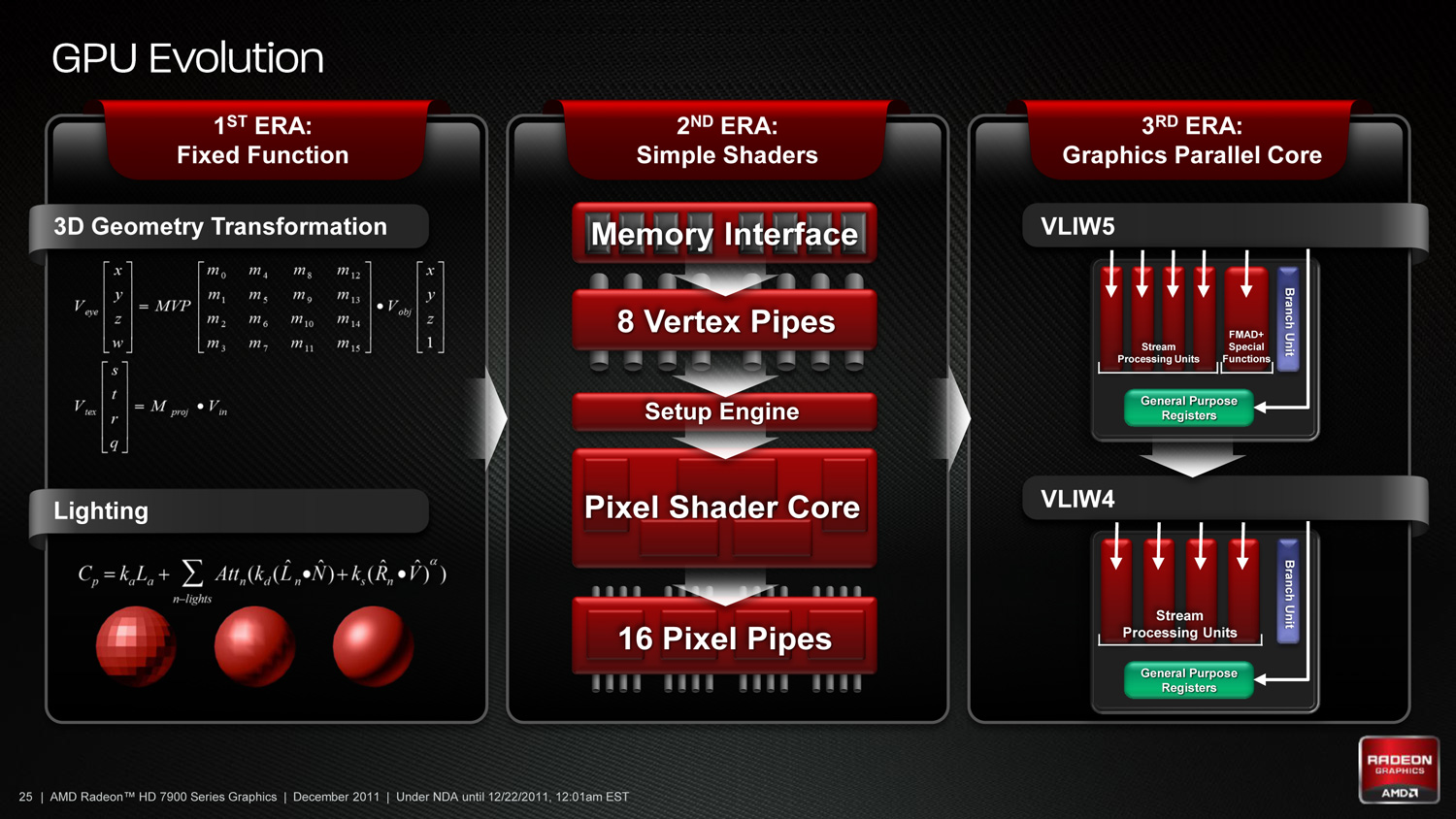
As we’ve already seen in some depth with the Radeon HD 6970,
VLIW architectures are very good for graphics work, but they’re poor
for compute work. VLIW designs excel in high instruction level
parallelism (ILP) use cases, which graphics falls under quite nicely
thanks to the fact that with most operations pixels and the color
component channels of pixels are independently addressable datum.
In
fact at the time of the Cayman launch AMD found that the average slot
utilization factor for shader programs on their VLIW5 architecture was
3.4 out of 5, reflecting the fact that most shader operations were
operating on pixels or other data types that could be scheduled together
Meanwhile, at a hardware level VLIW is a unique design in that it’s the
epitome of the “more is better” philosophy. AMD’s high steam processor
counts with VLIW4 and VLIW5 are a result of VLIW being a very thin type
of architecture that purposely uses many simple ALUs, as opposed to
fewer complex units (e.g. Fermi). Furthermore all of the scheduling for
VLIW is done in advance by the compiler, so VLIW designs are in effect
very dense collections of simple ALUs and cache.
The hardware traits of VLIW mean that for a VLIW architecture to work,
the workloads need to map well to the architecture. Complex operations
that the simple ALUs can’t handle are bad for VLIW, as are instructions
that aren’t trivial to schedule together due to dependencies or other
conflicts. As we’ve seen graphics operations do map well to VLIW, which
is why VLIW has been in use since the earliest pixel shader equipped
GPUs. Yet even then graphics operations don’t achieve perfect
utilization under VLIW, but that’s okay because VLIW designs are so
dense that it’s not a big problem if they’re operating at under full
efficiency.
When it comes to compute workloads however, the idiosyncrasies of VLIW
start to become a problem. “Compute” covers a wide range of workloads
and algorithms; graphics algorithms may be rigidly defined, but compute
workloads can be virtually anything. On the one hand there are compute
workloads such as password hashing that are every bit as embarrassingly
parallel as graphics workloads are, meaning these map well to existing
VLIW architectures. On the other hand there are tasks like texture
decompression which are parallel but not embarrassingly so, which means
they map poorly to VLIW architectures. At one extreme you have a highly
parallel workload, and at the other you have an almost serial workload.

Cayman, A VLIW4 Design
So long as you only want to handle the highly parallel workloads VLIW
is fine. But using VLIW as the basis of a compute architecture is going
is limit what tasks your processor is sufficiently good at. If you want
to handle a wider spectrum of compute workloads you need a more general
purpose architecture, and this is the situation AMD faced.
But why does AMD want to chase compute in the first place when they
already have a successful graphics GPU business? In the long term GCN
plays a big part in AMD’s Fusion plans, but in the short term there’s a
much simpler answer: because they have to.
In Q3’2011 NVIDIA’s Professional Solutions Business (Quadro + Tesla)
had an operating income of 95M on 230M in revenue. Their (consumer) GPU
business had an operating income of 146M, but on a much larger 644M in
revenue. Professional products have much higher profit margins and
it’s a growing business, particularly the GPU computing side. As it
stands NVIDIA and AMD may have relatively equal shares of the discrete
GPU market, but it’s NVIDIA that makes all the money. For AMD’s GPU
business it’s no longer enough to focus only on graphics, they need a
larger piece of the professional product market to survive and thrive in
the future. And thus we have GCN.
A Quick Refresher, Cont
Having established what’s bad about VLIW as a compute architecture,
let’s discuss what makes a good compute architecture. The most
fundamental aspect of compute is that developers want stable and
predictable performance, something that VLIW didn’t lend itself to
because it was dependency limited. Architectures that can’t work around
dependencies will see their performance vary due to those dependencies.
Consequently, if you want an architecture with stable performance that’s
going to be good for compute workloads then you want an architecture
that isn’t impacted by dependencies.
Ultimately dependencies and ILP go hand-in-hand. If you can extract ILP
from a workload, then your architecture is by definition bursty. An
architecture that can’t extract ILP may not be able to achieve the same
level of peak performance, but it will not burst and hence it will be
more consistent. This is the guiding principle behind NVIDIA’s Fermi
architecture; GF100/GF110 have no ability to extract ILP, and developers
love it for that reason.
So with those design goals in mind, let’s talk GCN.
VLIW is a traditional and well proven design for parallel processing.
But it is not the only traditional and well proven design for parallel
processing. For GCN AMD will be replacing VLIW with what’s fundamentally
a Single Instruction Multiple Data (SIMD) vector architecture (note:
technically VLIW is a subset of SIMD, but for the purposes of this
refresher we’re considering them to be different).

A Single GCN SIMD
At the most fundamental level AMD is still using simple ALUs, just like
Cayman before it. In GCN these ALUs are organized into a single SIMD
unit, the smallest unit of work for GCN. A SIMD is composed of 16 of
these ALUs, along with a 64KB register file for the SIMDs to keep data
in.
Above the individual SIMD we have a Compute Unit, the smallest fully
independent functional unit. A CU is composed of 4 SIMD units, a
hardware scheduler, a branch unit, L1 cache, a local date share, 4
texture units (each with 4 texture fetch load/store units), and a
special scalar unit. The scalar unit is responsible for all of the
arithmetic operations the simple ALUs can’t do or won’t do efficiently,
such as conditional statements (if/then) and transcendental operations.
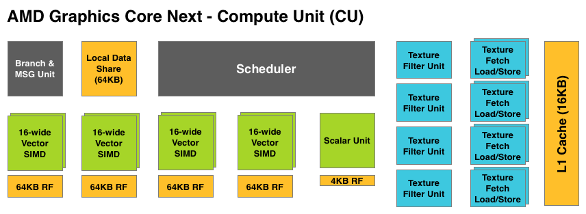
Because the smallest unit of work is the SIMD and a CU has 4 SIMDs, a
CU works on 4 different wavefronts at once. As wavefronts are still 64
operations wide, each cycle a SIMD will complete ¼ of the operations on
their respective wavefront, and after 4 cycles the current instruction
for the active wavefront is completed.
Cayman by comparison would attempt to execute multiple instructions from the same
wavefront in parallel, rather than executing a single instruction from
multiple wavefronts. This is where Cayman got bursty – if the
instructions were in any way dependent, Cayman would have to let some of
its ALUs go idle. GCN on the other hand does not face this issue,
because each SIMD handles single instructions from different wavefronts
they are in no way attempting to take advantage of ILP, and their
performance will be very consistent.
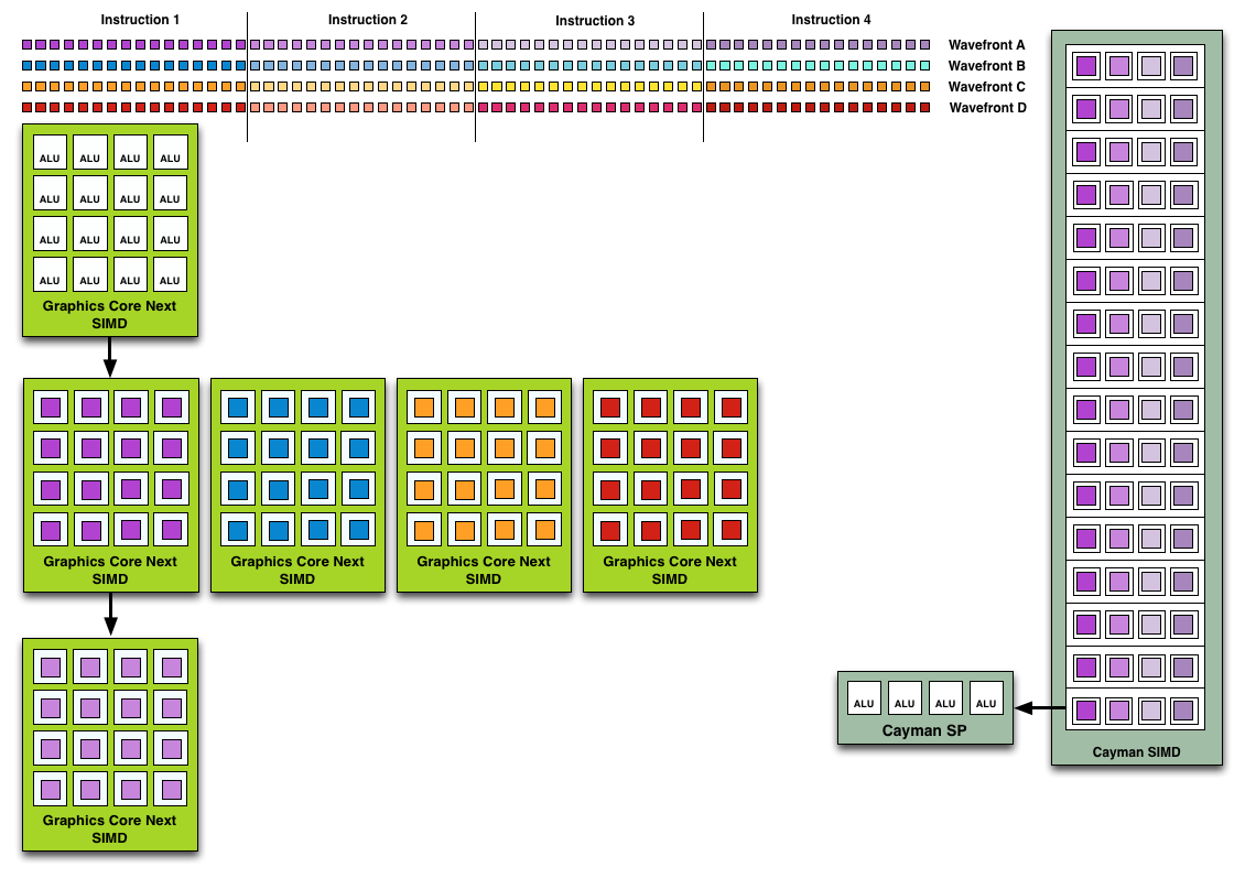
Wavefront Execution Example: SIMD vs. VLIW. Not To Scale - Wavefront Size 16
There are other aspects of GCN that influence its performance – the
scalar unit plays a huge part – but in comparison to Cayman, this is the
single biggest difference. By not taking advantage of ILP, but instead
taking advantage of Thread Level Parallism (TLP) in the form of
executing more wavefronts at once, GCN will be able to deliver high
compute performance and to do so consistently.
Bringing this all together, to make a complete GPU a number of these
GCN CUs will be combined with the rest of the parts we’re accustomed to
seeing on a GPU. A frontend is responsible for feeding the GPU, as it
contains both the command processors (ACEs) responsible for feeding the
CUs and the geometry engines responsible for geometry setup. Meanwhile
coming after the CUs will be the ROPs that handle the actual render
operations, the L2 cache, the memory controllers, and the various fixed
function controllers such as the display controllers, PCIe bus
controllers, Universal Video Decoder, and Video Codec Engine.
At the end of the day if AMD has done their homework GCN should
significantly improve compute performance relative to VLIW4 while gaming
performance should be just as good. Gaming shader operations will
execute across the CUs in a much different manner than they did across
VLIW, but they should do so at a similar speed. And for games that use
compute shaders, they should directly benefit from the compute
improvements. It’s by building out a GPU in this manner that AMD can
make an architecture that’s significantly better at compute without
sacrificing gaming performance, and this is why the resulting GCN
architecture is balanced for both compute and graphics.
Building Tahiti & The Southern Islands
Now that we’ve had a chance to go over the basis of the Graphics Core
Next architecture, let’s talk about the finished products.
Today AMD will be launching Tahiti, the first GPU of the Southern
Islands family. Southern Islands will initially be composed of 3 GPUs:
Tahiti, Pitcairn, and Cape Verde. Tahiti is the largest and most
powerful member of the Southern Islands family, while Pitcairn and Cape
Verde get progressively smaller. AMD has not yet announced the branding
or launch dates for Pitcarn and Cape Verde, but it typically takes AMD
around 6 months to launch a complete family. As such it’s reasonable to
expect that all 3 GPUs will have launched by the end of June although
there’s a good likelihood of it happening sooner than that.
All 3 GPUs are based on the GCN architecture, and as family members
will have similar features while varying the number of functional units
accordingly. Along with the architecture change Southern Islands brings
with it a slew of additional features that we’ll get to in the following
pages, including Partially Resident Texture (PRT) support, PCIe 3.0,
FastHDMI, Direct3D 11.1, and AMD’s fixed-function H.264 encoder, the
Video Codec Engine.
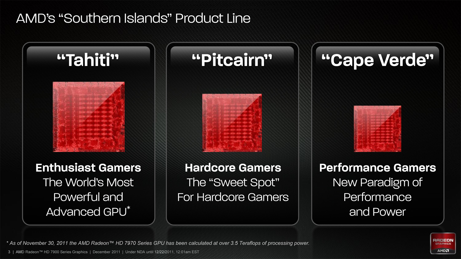
But today is all about Tahiti, so let’s get down to business.
As we quickly covered in our introduction, Tahiti is a 4.31B transistor
GPU based on the GCN architecture and built on TSMC’s new 28nm High-K
process. Due to TSMC canceling their 32nm process last year AMD has had
to wait over 2 years for the next full node rather than taking
advantage of the half-node process as they typically do, and as a result
the jump from Cayman at 40nm to Tahiti at 28nm is much bigger than with
past product launches. Whereas Cayman had 2.64B transistors and a die
size of 389mm2, Tahiti has a whopping 63% more transistors than Cayman
and yet it’s still smaller, coming in at a slightly more petite 365mm2.
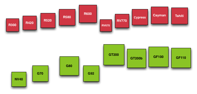
GPU Die Size Comparison
At this point AMD hasn’t provided us with the typical board power
values for 7970, but we do know that PowerTune is limited to 250W. In
terms of design 7970 is clearly intended to work in similar environments
as the 6970, in which case power consumption should be similar to the
6970.
Interestingly enough however we’re hearing that 7970 cards are proving
to be very overclockable, which is a good sign for the state of TSMC’s
28nm process, and at the same time a bit distressing. Moore’s Law has
continued to hold with respect to transistor density, but the power
consumption benefits of using smaller nodes has continued to wane.
Having a lot of overclocking headroom means that the 7970 has the
potential to be much faster, but it also means that the 7970 (and 28nm
GPUs in general) are going to be bottlenecked by power. In which case
seeing as how we’re already approaching 300W with single-GPU video
cards, the performance gains realized from future fabrication processes
would be limited to the ever diminishing returns on power consumption
improvements.
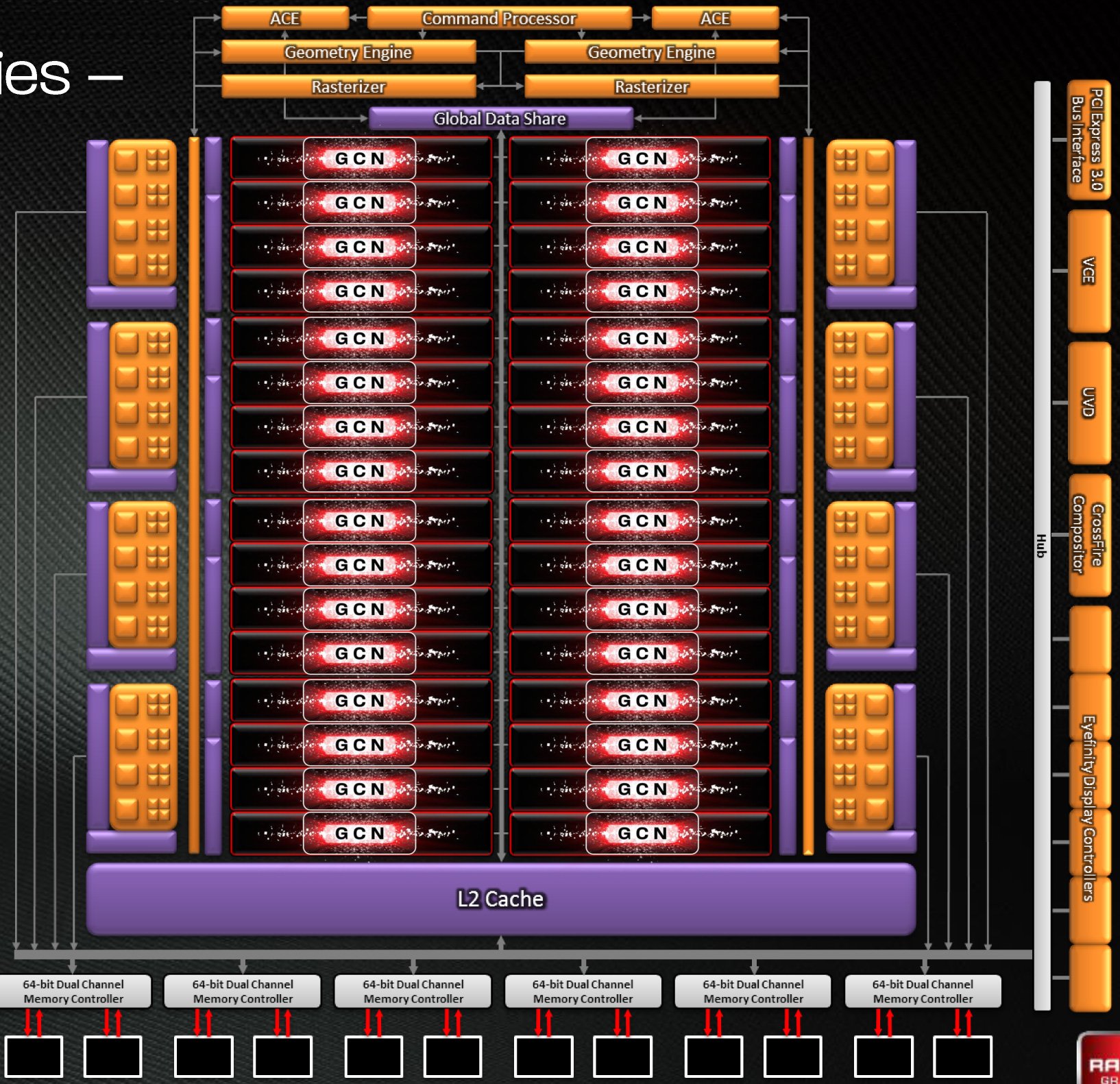
Diving deeper into Tahiti, as per the GCN architecture Tahiti’s 2048
SPs are organized into 32 Compute Units. Each of these CUs contains 4
texture units and 4 SIMD units, along with a scalar unit and the
appropriate cache and registers. At the 7970’s core clock of 925MHz this
puts Tahiti’s theoretical FP32 compute performance at 3.79TFLOPs, while
its FP64 performance is ¼ that at 947MFLOPs. As GCN’s FP64 performance
can be configured for 1/16, ¼, or ½ its FP32 performance it’s not clear
at this time whether the 7970’s ¼ rate was a hardware design decision
for Tahiti or a software cap that’s specific to the 7970. However as
it’s obvious that Tahiti is destined to end up in a FireStream card we
will no doubt find out soon enough.
Meanwhile the frontend/command processor for Tahiti is composed of 2
Asynchronous Command Engines (ACEs) and 2 geometry engines. Just as with
Cayman each geometry engine can dispatch 1 triangle per clock, giving
Tahiti the same theoretical 2 triangle/clock rate as Cayman. As we’ll
see however, in practice Tahiti will be much faster than Cayman here due
to efficiency improvements.
Looking beyond the frontend and shader cores, we’ve seen a very
interesting reorganization of the rest of the GPU as opposed to Cayman.
Keeping in mind that AMD’s diagrams are logical diagrams rather than
physical diagrams, the fact that the ROPs on Tahiti are not located near
the L2 cache and memory controllers in the diagram is not an error. The
ROPs have in fact been partially decoupled from the L2 cache and memory
controllers, which is also why there are 8 ROP partitions but only 6
memory controllers. Traditionally the ROPs, L2 cache, and memory
controllers have all been tightly integrated as ROP operations are
extremely bandwidth intensive, making this a very design for AMD to use.
As it turns out, there’s a very good reason that AMD went this route.
ROP operations are extremely bandwidth intensive, so much so that even
when pairing up ROPs with memory controllers, the ROPs are often still
starved of memory bandwidth. With Cayman AMD was not able to reach their
peak theoretical ROP throughput even in synthetic tests, never mind in
real-world usage. With Tahiti AMD would need to improve their ROP
throughput one way or another to keep pace with future games, but
because of the low efficiency of their existing ROPs they didn’t need to
add any more ROP hardware, they merely needed to improve the efficiency
of what they already had.
The solution to that was rather counter-intuitive: decouple the ROPs
from the memory controllers. By servicing the ROPs through a crossbar
AMD can hold the number of ROPs constant at 32 while increasing the
width of the memory bus by 50%. The end result is that the same number
of ROPs perform better by having access to the additional bandwidth they
need.

The big question right now, and one we don’t have an answer to, is what
were the tradeoffs for decoupling the ROPs? Clearly the crossbar design
has improved ROP performance through the amount of memory bandwidth
they can access, but did it impact anything else? The most obvious
tradeoff here would be for potentially higher latency, but there may be
other aspects that we haven’t realized yet.
On that note, let’s discuss the memory controllers quickly. Tahiti’s
memory controllers aren’t significantly different from Cayman’s but
there are more of them, 50% more in fact, forming a 384bit memory bus.
AMD has long shied away from non-power of 2 memory busses, and indeed
the last time they even had a memory bus bigger than 256bits was with
the ill-fated 2900XT, but at this point in time AMD has already nearly
reached the practical limits of GDDR5. AMD’s ROPs needed more memory
bandwidth, but even more than that AMD needed more memory bandwidth to
ensure Tahiti had competitive compute performance, and as such they had
little choice but to widen their memory bus to 384bits wide by adding
another 2 memory controllers.
It’s worth noting though that the addition of 2 more memory controllers
also improves AMD’s cache situation. With 128KB of L2 cache being tied
to each memory controller, the additional controllers gave AMD 768KB of
L2 cache, rather than the 512KB that a 256bit memory bus would be paired
with.
source:http://www.anandtech.com