Pages

19 September 2012

Rosewill Fortress Platinum 450W

Rosewill is a familiar name here at AnandTech. It's Newegg's in-house brand, through which they sell products such as notebook accessories, peripheral equipment, cases and power supplies. Their stated goal is to "bring quality hardware and affordable prices together". In most cases they really care about the pricing, but today we will review one of their more expensive high-class offerings. Not long ago we tested their Gold PSUs, which also belong to this classification; the new products go one step further.
The Fortress series from Rosewill has four different versions, all with 80 Plus Platinum certification and non-modular cables. We'll be focusing on the 450W model in this article as this rating is interesting for the largest number of potential buyers. Japanese capacitors and a single 12V output are just two out of many features. Let’s see how the unit performs and whether it is able to surpass their Capstone series.

Gigabyte Z77X-UP4 TH Review: Thunderbolt Times Two


Now that the exclusive license Apple had for Thunderbolt has expired, since Computex 2012 we have seen a number of motherboards destined for PCs with a Thunderbolt connector.  Thunderbolt on a motherboard is still an added luxury, adding some $40 to the cost of the board to the user, though that can pale in comparison to the cost of Thunderbolt devices and storage.  Despite all this, Gigabyte’s foray into the Thunderbolt world is initiated in part by the board we are reviewing today – the 
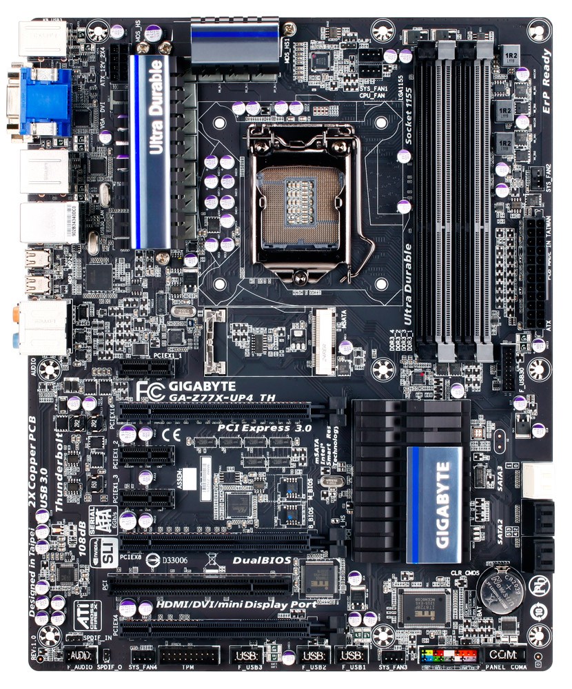
Gigabyte Z77X-UP4 TH.  Using the Z77 chipset we get a motherboard with two Thunderbolt ports, but it also has the enhanced power delivery brought about by Ultra Durable 5.

Gigabyte Z77X-UP4 TH Overview
Like many Gigabyte boards in the Z77 range, there are very few issues with the Ivy Bridge platform in Gigabyte’s hands.  Due to MultiCore Enhancement, CPU performance matches that of other Gigabyte and ASUS products this generation, and the Z77X-UP4 TH comes with the two major additions – a two port Thunderbolt controller, and IR3550 ICs to help with the power delivery.  As we saw on the Gigabyte X79S-UP5, these ICs do help with power consumption assuming the cost can be justified.

Visually, the board does look a little empty with smaller heatsinks, a gap left for an mSATA drive and some empty IO, but we do have a classic three-way PCIe device implementation such that with an Ivy Bridge processor, the board can run x16/-/-, x8/x8/- or x8/x4/x4 in PCIe 3.0 mode.  We lack any extra SATA ports, with only those provided by the chipset being used, and the back panel uses only USB 3.0 – two from the chipset and four from a VIA VL800 controller.  The other two USB 3.0 ports that the chipset provide are used for an onboard USB 3.0 header.

In terms of extra hardware and controllers beyond the chipset standard, we are hard pushed to find anything special beyond the Thunderbolt controller – sure there is a USB 3.0 VIA VL800 chip, but the audio is a Realtek ALC892 and the Ethernet is a Realtek 8111.  The iTE chips onboard give us access to a combination PS/2 port and a COM port as well.  But the lack of extra SATA ports is perhaps a little strange for a UP4 product.

Performance on the Z77X-UP4 TH comes on par with the other Gigabyte motherboards tested.  This is due to the fact that the Z77X-UP4 TH enables MultiCore Enhancement when XMP is enabled, as per our standard testing methodology.  This gives our test bed an extra 200 MHz under full threaded load, which benefits all CPU intensive tasks.  Power consumption, due to the use of IR3550 ICs, is low compared to most Z77 motherboards we have tested, and the third PCIe 3.0 slot at performs well with a PCIe 3.0 GPU plugged in.

The only question mark comes down to the price.  Thunderbolt and Ultra Durable 5 are, to quote a famous brand, ‘reassuringly expensive’.  Thunderbolt adoption in the PC market is quite low right now due to the lack of competitive pricing, so having two ports on board for up to twelve devices is a bit overkill.  This limits the Z77X-UP4 TH more into a niche target segment.  Though if you have 6-12 TB devices, then this is a nice board to consider.  For all other usage scenarios, your $190-$200 might be worth investing in a Z77X-UD5H.

Visual Inspection
One of the benefits of using the IR3550 ICs in the power delivery is that because each one is rated up to 60 amps, this means fewer phases are needed on board.  Having fewer phases means saving energy and cost, but also results in smaller heatsinks, especially when we consider the IR3550s have unique IP to help keep cool.  This reduction in the number of phases along with the smaller heatsinks gives the socket area of the Z77X-UP4 TH a lot of room.  Almost every air cooler under the sun should fit on this motherboard, even a NoFan.  (Actually, the NoFan will probably impinge on the memory slots, requiring low profile memory).

09 March 2012

PowerColor Radeon HD 7770 1 GB

Introducing  PowerColor Radeon HD 7770 1 GB

Introduction


Launched amongst much fanfare earlier this year, It's now time for AMD's Graphics CoreNext architecture to get down to serious business: driving a mainstream GPU that offers killer value at price-points which most people will end up buying. AMD today launched the Radeon HD 7700 series, based on its spanking new silicon codenamed "Cape Verde".


What makes this launch a particularly monumental challenge for Graphics CoreNext is that it now has to deliver on its biggest design goal, that of being a more efficient number-cruncher than previous-generation VLIW architecture. This efficiency is supposed to show in relative performance per mm² (taking the new 28 nm fab process into account), performance per Watt, and in more layman terms, performance to stream processor count.

But first, a little history lesson. AMD addressed the sub-$200 market with its first DirectX 11 generation of GPUs using the Radeon HD 5700 series, based on the 40 nm "Juniper" silicon. Since the following HD 6000 series was also based on this process, and AMD had achieved higher performance targets with "Barts", it decided to reshuffle the higher-end lineup, give Barts the HD 6800 series, and since Juniper was the only GPU smaller than Barts, re-brand it to the HD 6700 series, to everyone's disgust including ours. With the transition to the new 28 nm fab process and a new number-chomping architecture, Graphics CoreNext, designing a new GPU became inevitable for AMD. Hence, Cape Verde. Products based on this chip, the Radeon HD 7770 and Radeon HD 7750, are touted to be true successors of the HD 6700 series.


We also have the following reviews for you today:

Architecture

Cape Verde is a downscale from the "Tahiti" silicon, on which higher Radeon HD 7900 series parts are based. There are fewer number of redundant components, so Cape Verde is left functionally-identical to Tahiti, but is smaller, built for more affordable graphics cards. Cape Verde also retains the basic hierarchy of the architecture as implemented in Tahiti. A command processor takes input from the host machine, decodes them, and does the groundwork for the number-crunching area, the Graphics CoreNext clusters, which then perform all the shader and math-intensive processing. The Raster Operations area does the final leg of the processing, and the information is forwarded to the display logic. All components are interconnected to an L2 cache, that works as a very fast scratchpad for the GPU, and of course, the memory controllers.


Cape Verde has 10 Graphics CoreNext Computing Units (GCN CUs), which total up 640 stream processors. The chip has 40 TMUs, and 16 ROPs. It features a 128-bit wide GDDR5 memory interface, with which it communicates with 1 GB of memory. The chip retains the display logic of Tahiti, which lets you connect up to 6 displays in Eyefinity for productivity usage. The GPU also features PCI-Express Gen. 3.0 support, which increases bandwidth between it and the rest of the system. While we doubt the chip really needs 32 GB/s of system bandwidth, PCIe Gen 3.0 could come handy when connected in configurations with lower number of PCIe lanes (such as x8, x4, or even x1), as PCIe Gen 3.0 has more bandwidth per lane.


With the new HD 7000 series, AMD also introduced what it refers to as ZeroCore Technology. Simply put, this feature reduces power consumption of the GPU down to zero, by gating power to it, when the system is idling for extended periods of time, when the displays are blanked. In this power state, the graphics card draws less than 3W of power, making it extremely energy-efficient. The typical board power figures for the Radeon HD 7700 GPUs are also claimed by its makers to be extremely low.

PowerColor HD 7770 1 GB


PowerColor sent us a card that is pretty much identical to the AMD reference design. Only the cooler has undergone very minor changes on the outside. Its internals are the same as on the AMD board, clock speeds are also at reference design level.

Packaging


Contents


You will receive:
  • Graphics card
  • Driver CD + Documentation
  • Analog VGA Adapter
  • Mini-DP to DP Adapter

MSI Radeon HD 7770 OC 1 GB

Introducing MSI Radeon HD 7770 OC 1 GB

Introduction


Launched amongst much fanfare earlier this year, It's now time for AMD's Graphics CoreNext architecture to get down to serious business: driving a mainstream GPU that offers killer value at price-points which most people will end up buying. AMD today launched the Radeon HD 7700 series, based on its spanking new silicon codenamed "Cape Verde".


What makes this launch a particularly monumental challenge for Graphics CoreNext is that it now has to deliver on its biggest design goal, that of being a more efficient number-cruncher than previous-generation VLIW architecture. This efficiency is supposed to show in relative performance per mm² (taking the new 28 nm fab process into account), performance per Watt, and in more layman terms, performance to stream processor count.

But first, a little history lesson. AMD addressed the sub-$200 market with its first DirectX 11 generation of GPUs using the Radeon HD 5700 series, based on the 40 nm "Juniper" silicon. Since the following HD 6000 series was also based on this process, and AMD had achieved higher performance targets with "Barts", it decided to reshuffle the higher-end lineup, give Barts the HD 6800 series, and since Juniper was the only GPU smaller than Barts, re-brand it to the HD 6700 series, to everyone's disgust including ours. With the transition to the new 28 nm fab process and a new number-chomping architecture, Graphics CoreNext, designing a new GPU became inevitable for AMD. Hence, Cape Verde. Products based on this chip, the Radeon HD 7770 and Radeon HD 7750, are touted to be true successors of the HD 6700 series.


We also have the following reviews for you today:

Architecture

Cape Verde is a downscale from the "Tahiti" silicon, on which higher Radeon HD 7900 series parts are based. There are fewer number of redundant components, so Cape Verde is left functionally-identical to Tahiti, but is smaller, built for more affordable graphics cards. Cape Verde also retains the basic hierarchy of the architecture as implemented in Tahiti. A command processor takes input from the host machine, decodes them, and does the groundwork for the number-crunching area, the Graphics CoreNext clusters, which then perform all the shader and math-intensive processing. The Raster Operations area does the final leg of the processing, and the information is forwarded to the display logic. All components are interconnected to an L2 cache, that works as a very fast scratchpad for the GPU, and of course, the memory controllers.


Cape Verde has 10 Graphics CoreNext Computing Units (GCN CUs), which total up 640 stream processors. The chip has 40 TMUs, and 16 ROPs. It features a 128-bit wide GDDR5 memory interface, with which it communicates with 1 GB of memory. The chip retains the display logic of Tahiti, which lets you connect up to 6 displays in Eyefinity for productivity usage. The GPU also features PCI-Express Gen. 3.0 support, which increases bandwidth between it and the rest of the system. While we doubt the chip really needs 32 GB/s of system bandwidth, PCIe Gen 3.0 could come handy when connected in configurations with lower number of PCIe lanes (such as x8, x4, or even x1), as PCIe Gen 3.0 has more bandwidth per lane.


With the new HD 7000 series, AMD also introduced what it refers to as ZeroCore Technology. Simply put, this feature reduces power consumption of the GPU down to zero, by gating power to it, when the system is idling for extended periods of time, when the displays are blanked. In this power state, the graphics card draws less than 3W of power, making it extremely energy-efficient. The typical board power figures for the Radeon HD 7700 GPUs are also claimed by its makers to be extremely low.

MSI Radeon HD 7770 OC 1 GB


MSI has equipped their card with a new cooling solution that uses a dual fan design. In terms of clock speed we see a small bump, but not as big as on other overclocked cards today.

Packaging


Contents


You will receive:
  • Graphics card
  • Driver CD + Documentation
  • PCI-Express Power Cable
  • Mini-DP to DP Adapter
 

XFX HD 7770 Black Edition Super Overclock 1 GB

Introducing XFX HD 7770 Black Edition Super Overclock 1 GB

Introduction


Launched amongst much fanfare earlier this year, It's now time for AMD's Graphics CoreNext architecture to get down to serious business: driving a mainstream GPU that offers killer value at price-points which most people will end up buying. AMD today launched the Radeon HD 7700 series, based on its spanking new silicon codenamed "Cape Verde".


What makes this launch a particularly monumental challenge for Graphics CoreNext is that it now has to deliver on its biggest design goal, that of being a more efficient number-cruncher than previous-generation VLIW architecture. This efficiency is supposed to show in relative performance per mm² (taking the new 28 nm fab process into account), performance per Watt, and in more layman terms, performance to stream processor count.

But first, a little history lesson. AMD addressed the sub-$200 market with its first DirectX 11 generation of GPUs using the Radeon HD 5700 series, based on the 40 nm "Juniper" silicon. Since the following HD 6000 series was also based on this process, and AMD had achieved higher performance targets with "Barts", it decided to reshuffle the higher-end lineup, give Barts the HD 6800 series, and since Juniper was the only GPU smaller than Barts, re-brand it to the HD 6700 series, to everyone's disgust including ours. With the transition to the new 28 nm fab process and a new number-chomping architecture, Graphics CoreNext, designing a new GPU became inevitable for AMD. Hence, Cape Verde. Products based on this chip, the Radeon HD 7770 and Radeon HD 7750, are touted to be true successors of the HD 6700 series.


We also have the following reviews for you today:

Architecture

Cape Verde is a downscale from the "Tahiti" silicon, on which higher Radeon HD 7900 series parts are based. There are fewer number of redundant components, so Cape Verde is left functionally-identical to Tahiti, but is smaller, built for more affordable graphics cards. Cape Verde also retains the basic hierarchy of the architecture as implemented in Tahiti. A command processor takes input from the host machine, decodes them, and does the groundwork for the number-crunching area, the Graphics CoreNext clusters, which then perform all the shader and math-intensive processing. The Raster Operations area does the final leg of the processing, and the information is forwarded to the display logic. All components are interconnected to an L2 cache, that works as a very fast scratchpad for the GPU, and of course, the memory controllers.


Cape Verde has 10 Graphics CoreNext Computing Units (GCN CUs), which total up 640 stream processors. The chip has 40 TMUs, and 16 ROPs. It features a 128-bit wide GDDR5 memory interface, with which it communicates with 1 GB of memory. The chip retains the display logic of Tahiti, which lets you connect up to 6 displays in Eyefinity for productivity usage. The GPU also features PCI-Express Gen. 3.0 support, which increases bandwidth between it and the rest of the system. While we doubt the chip really needs 32 GB/s of system bandwidth, PCIe Gen 3.0 could come handy when connected in configurations with lower number of PCIe lanes (such as x8, x4, or even x1), as PCIe Gen 3.0 has more bandwidth per lane.


With the new HD 7000 series, AMD also introduced what it refers to as ZeroCore Technology. Simply put, this feature reduces power consumption of the GPU down to zero, by gating power to it, when the system is idling for extended periods of time, when the displays are blanked. In this power state, the graphics card draws less than 3W of power, making it extremely energy-efficient. The typical board power figures for the Radeon HD 7700 GPUs are also claimed by its makers to be extremely low.

XFX HD 7770 Black Edition Super Overclock


XFX has done extensive cooling changes to their card. We see a similar cooler design as on the company's HD 7900 Series - just a smaller version. XFX has given their card the biggest clock increase of all HD 7770 cards reviewed today, but these changes come at a premium, the card will retail at $179.

AMD Radeon HD 7850 & HD 7870 2 GB

Introducing AMD Radeon HD 7850 & HD 7870 2 GB


"Next-generation", "Graphics CoreNext", "Radeon HD 7000 series", "Southern Islands"...this is it. AMD's new GPU architecture has moved into the phase where its makers launch serious money-making products based on it, with the Radeon HD 7800 series.


Targeting a wide price-range between $250-$350, the HD 7800 series falls into the market-segment both AMD and NVIDIA have known to refer to as the "sweetspot" segment. When people decide to turn their $400 Dell desktops into gaming PCs, instead of buying $300 game consoles for their TV, it's graphics cards from this segment that they end up buying. Smooth gameplay at full-HD resolution is a requisite.

AMD has to get several things right about the products it's launching today, because the competitiveness of the entire HD 7000 series hangs on its success. First, it needs to create a sizable performance jump, over the previous-generation Radeon HD 6800 series; second, its new chip has to prove Graphics CoreNext as being a viable investment for AMD by meeting some basic cost/performance, performance/die-area, and performance/Watt figures. VLIW4 had a very short stint before Graphics CoreNext.


NVIDIA hasn't even started with its next-generation GPU lineup, leaving its previous-generation to defend itself against a reinvigorated AMD lineup. AMD appears to have exploited this late-coming by NVIDIA. The launch prices of Radeon HD 7900 series resembled those of NVIDIA's high-end GTX series, the Radeon HD 7700 series products ask a couple of dozen Dollars too many. AMD kept the theme going with the Radeon HD 7800 series. You may recollect AMD's Radeon HD 6870 shipping for $240 on launch, and the HD 6850 for $180, both very attractive prices. The slide above is every indication of AMD trying to justify launch prices of $349 for the HD 7870 and $249 for the HD 7850, just because they are touted to outperform whatever NVIDIA currently has in those price-ranges (we're going to find that out in this review).

Architecture

The Radeon HD 7800 series consists of two models, the Radeon HD 7870, and the Radeon HD 7850, both stretched far apart in the market segment. The two are based on AMD's brand new GPU, codenamed "Pitcairn". Built on the 28 nm fabrication process, this new chip holds 2.8 billion transistors. "Pitcairn" is a 100% upscale of the "Cape Verde" silicon, on which the Radeon HD 7700 series is based. It has 1280 Graphics CoreNext stream processors, arranged in 20 Graphics CoreNext Compute Units (GCN CUs). The component hierachy of "Pitcairn" resembles that of "Tahiti", more than it does "Cape Verde". The 20 GCN CUs are arranged in two clusters, with two sets of geometry processing engines, and rasterizers, handing the initial stages of graphics processing.

Apart from 1280 stream processors, Pitcairn has 80 Texture Memory Units (TMUs), 32 ROPs (Raster Operations), and a 256-bit wide GDDR5 memory interface, holding 2 GB of memory. Here's something interesting. AMD deemed 2 GB as the new standard memory amount for performance-segment graphics cards. Both the HD 7870 and HD 7850 have 2 GB of memory, clocked at 1200 MHz (4.80 GHz GDDR5 effective), churning out 153.6 GB/s memory bandwidth. As for the core clock, the HD 7870 has its core clocked at 1000 MHz, making it AMD's second "GHz Edition" SKU after the HD 7770; while the HD 7850 has its core clocked at 860 MHz. The Radeon HD 7850 is carved out by disabling four GCN CUs, leaving 1024 stream processors, and 64 TMUs. The rest of the SKU is identical to the HD 7870.

In this review, we are evaluating both the Radeon HD 7870 and the Radeon HD 7850. Both cards are AMD reference design samples provided by the company.

ASUS Radeon HD 7750 1 GB

Introducing ASUS Radeon HD 7750 1 GB.
Two weeks ago AMD launched their Radeon HD 7700 Series. The cards use the all-new Cape Verde graphics processor which is based on AMD's new GCN Graphics Core Next architecture that promises increased performance and lower power draw.

Cape Verde is a downscale from the "Tahiti" silicon, on which higher Radeon HD 7900 series parts are based. There are fewer number of redundant components, so Cape Verde is left functionally-identical to Tahiti, but is smaller, built for more affordable graphics cards. Cape Verde also retains the basic hierarchy of the architecture as implemented in Tahiti.


The ASUS Radeon HD 7750 is a custom implementation of the HD 7750, using a custom heatsink and increased clock rates of 820 MHz GPU and 1150 MHz memory.

Packaging


Contents


You will receive:
  • Graphics card
  • Driver CD + Documentation
  • Analog VGA Adapter


Samsung 30 nm Green PC3-12800 Low Profile 1.35 V DDR3

Introducing

Over the past couple of months, there's been quite an uproar on various tech forums about Samsung's latest 30 nm Low-Power "Green" DDR3. During the time since they were "discovered", we've seen reports of 1600 MHz sticks hitting 2400 MHz and more, a healthy 50%+ overclock ability that in today's memory market is very near unheard of. Non-plussed, I managed to source a sample to take a look, and investigate the hype. Here's what Samsung has to say about their latest Low Power "Green" DDR3 on their website:
 

First in the Market with Advanced DDR3

Double Data Rate Three, Synchronous DRAM, or DDR3, is the new generation of high performance, ultra-low-power memory interface technology used in high performance servers, desktops and notebooks. As the number one supplier in memory, Samsung continues to lead the industry with cutting-edge SDRAM products from the first DDR in 1997, DDR2 in 2001 and DDR3 in 2005. Samsung's high performance main memory solutions are based on JEDEC standards and leverage the company's leadership in advanced research and development of semiconductor process technology.

Samsung's DDR3 brings new levels of performance to notebooks, desktops and servers and pushes the envelope in key areas like power consumption, speed and bandwidth. Our recent 30nm class, 1.35V, 2Gb DDR3 is the world's first ultra-low-power memory technology, with more than a 76% power savings over traditional DDR2 at 2x the bandwidth. When you're ready to make a move to DDR3 or are considering upgrading your systems, we're here to provide the best optimal solution for enhancing your competitive edge.

As far as I am aware of, Samsung hasn't had a memory product that excited enthusiasts since the release of their 1.8v HCF0 ICs, which although decent overclockers, were eclipsed by other products on the market that went just that much further. Of course, those HCF0 weren't 30nm, nor were they rated for operation at 1.35 V. Are these new sticks worth the hype the receive?